JFET Full Form
What is the Full Form of JFET?
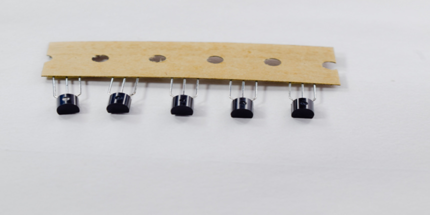
Junction Field Effect Transistor which is also known as JFET, is a unipolar device in which the action of an electric field at a reverse-biased pn-junction regulates the current passage between its two electrodes. The majority of carriers in a JFET flow down a narrow "Channel", which is a semiconductor material of high resistivity of either N-type or P-type silicon, which is formed without any PN-junctions and has two ohmic electrical connections at either end that are typically referred to as the Drain and the Source. One of the most basic varieties of the field-effect transistor is the Junction field-effect transistor. JFETs are voltage-controlled electronics, in contrast to the Bipolar Junction Transistor. The majority of charge carriers in JFETs are responsible for the current flow. However, the majority and minority charge carriers contribute to the current flow in BJTs. JFETs are unidirectional because the bulk of charge carriers are the only ones responsible for the current flow.
- What is the Full Form of JFET?
- JFET Configurations
- Applications of JFET
- Advantages of JFET
- Disadvantages of JFET
JFET Configurations
There are two types of configurations for JFET transistors.
N-Channel JFET
P-Channel JFET

The channel of an N-channel JFET is doped with donor impurities, causing electrons, i.e. flow of current flow through the channel negatively hence getting the name N-channel JFET.
The P-channel JFET channel is doped with acceptor impurities, resulting in positive current flow across the channel in holes (hence the name P-channel). Due to the higher mobility of electrons via a conductor than holes, N-channel JFETs offer higher channel conductivity (lower resistance) than P-channel JFETs. Due to this, N-channel JFETs are more effective conductors than P-channel JFETs.
At either end of the channel, there are two ohmic electrical connections known as the Drain and the Source. The Gate terminal, which can also be of P-type or N-type material and forms a PN-junction with the main channel, is a third electrical connection within this channel.
Applications of JFET
JFET can be used as:
A continual source of current
Buffer amplifier
Electronic switch
Phase shift oscillator
high impedance wide band amplifier
voltage development resistor (VDR)
voltage variable resistor (VVR) or
chopper
Advantages of JFET
They have greater thermal stability since it has a negative temperature coefficient of resistance.
High impedance
Low power consumption
JFETs can be made into small sizes, thereby occupying less circuit space.
They have less noise as JFETs are the majority of charge carriers.
Disadvantages of JFET
The Relatively low gain-bandwidth product
As frequency increases, JFET performance declines due to internal capacitance feedback.
Frequently Asked Questions (FAQs)
JFET was invented in 1953.
Transconductance (gm)
AC Drain Resistance (rd)
Amplification Factor (µ)
Because the gate voltage controls the drain current in JFET, it is referred to as a voltage-controlled device.
These components are excellent switches due to their high input impedance. However, MOSFETs have a substantially higher input impedance (~10^10 to 10^15Ω) than JFETs (~10^8Ω) due to their insulated gate. Hence MOSFETS are preferred over JFETs as digital switches.
JFET is a three-terminal device which works only in depletion mode, while MOSFET is a four-terminal device which works in both depletion and enhancement modes.

Student Community: Where Questions Find Answers