PCB Full Form
What is the full form of PCB?
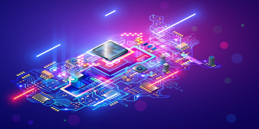
Printed circuit boards are PCBs in their complete form. A printed circuit board, or PCB for short, serves as the structure on which an electrical circuit is built. A layout for the circuit configuration is present on a PCB. Connecting electrical components is supported mechanically by it.
The components of a printed circuit board (PCB) are termed to be non-conductive. PCBs are available in a variety of shapes, sizes, and types. A PCB is used to install and link radio equipment, resistors, diodes, capacitors, and semiconductors. Computers, televisions, tablets, laptops, smartphones, smartwatches, and other electronic devices are all dependent on PCBs.
- What is the full form of PCB?
- Types of PCB
- Composition of PCB
- Advantages of PCB
Types of PCB
The most typical PCBs are those that are constructed on rigid substrates. Other circuit board types, on the other hand, can be built from a variety of materials. Common varieties of these include:
1. Single-sided: Only one surface of this board is used to install components. Usually, a solder mask is applied on the totally copper (ground) rear surface.
Circuit boards that are double-sided have components installed on both surfaces. The surfaces will have traces that carry signals between components since each surface is defined as a signal layer in the PCB stack-up.
2. Multi-layer PCBs - These circuit boards either have conductive plane layers or conductors on the internal layers that transfer electrical impulses between components. PCBs with many layers might be single-sided or multi-layered.
3. Rigid-flex PCBs - In a printed circuit board assembly, rigid-flex PCBs join two or more rigid parts together using a flexible polyimide ribbon. When the design needs to incorporate a moveable component, like a folding or bending enclosure, a rigid-flex board may be used.
Fully flexible printed circuit boards (PCBs) are composed entirely of flexible polyimide ribbons and do not contain any hard components. In the same way that rigid and rigid-flex printed circuit boards can have components mounted and soldered on them, so can these boards.
In order to provide far better rigidity and heat dissipation than traditional rigid printed circuit boards, metal-core PCBs incorporate a metal slab in the core layer, often aluminium. The rigid PCB manufacturing process is very different from the metal-core PCB manufacturing process.
There are a few design considerations to take into account to ensure solvability because the metal-core PCB manufacturing process differs significantly from the traditional rigid PCB manufacturing process. High-power lighting and some industrial applications frequently use these boards.
4. Ceramic PCBs - Less frequently employed, these boards are used in applications requiring extremely high thermal conductivity so that the board can effectively disperse significant amounts of heat away from components.
Composition of PCB
To accomplish the desired connectivity of the circuit, a single PCB is made of a variety of materials. PCB materials include the following:
Building non : conductive bases use fibreglass and plastic substrates.
Copper: laminated for electrical conductivity on one or both sides of the plastic or fibreglass substrate.
Soldermask: It is primarily made to protect copper circuits on the outer layers from oxidation by isolating them.
Nomenclature Ink: After the solder mask has been layered, it is printed with identifying details, marks, and barcodes. The term nomenclature refers to these markers.
Advantages of PCB
PCBs can be used in several electronic circuit types. It also has a number of benefits, including:
For use in many current products, this design is compact and lightweight.
Reliability
Maintaining simplicity in complex systems.
Because of their low production costs, PCBs are very economical.
Minimal chance of short circuits
Re-workable
Durable
High complexity in circuits