PCBs Full Form
What is the full form of PCBs?
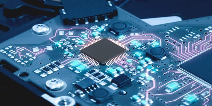
The complete form of PCBs is a Printed Circuit Board. Also called Printed Wiring Board (PWB), is a medium used in electrical engineering that steadily connects electronic components. Printed circuit boards are used in nearly all electronic products including Televisions, Personal Computers, Laptops and even Smartphones. Alternatives of PCBs are wire wraps and end-to-end construction systems, both were once popular in use but are now rarely preferred.
- What is the full form of PCBs?
- Printed Circuit Board
- History of PCBs
- Applications of PCBs
- Benefits of PCBs
- Limitations of PCBs

Printed Circuit Board
Printed circuit boards are used in nearly all electronic products. It is in the form of a laminated sandwich structure of a conductive layer, each of which is designed with a pattern of traces, planes, and other features (as wires are on a flat surface). Engraved from one or more sheet layers of copper laminated between sheet layers of a non-conductor substrate. Electrical components may be designated to conductive pads on the outer layers in the shape devised to accept the component's terminals, generally through soldering to electrically connect and mechanically bind them to it.
PCBs require additional designing effort to lay out the circuit, but their manufacturing and assembly can be automated. Also, Electronic Design Automation Software is available that performs most of the layout and design tasks. They can also be made manually in small quantities but they provide fewer benefits.
History of PCBs
Before the development of printed circuit boards, electrical circuits were joined end-to-end on a chassis which was a plain metal frame or pan.
The development of modern printed circuit boards started early in the 20th century, when in 1903, a German inventor, Albert Hanson laminated flat foil conductors to an insulating board, in multiple layers.
Thomas Edison, in 1904, experimented with plating conductors onto linen paper by chemical procedures.
Later in 1913, Arthur Berry patented a print-and-etch method in the UK. Followed by the patent of the flame-spray metal method by Max Schoop in the United States.
Applications of PCBs
PCBs are used in almost every electronic devices which are used in different industries, or home appliances or anywhere.
PCBs are used in fields of Biomedical engineering, replacing their typical alternatives, all because of their copper layering.
PCBs are being used in fabricating sensors, such as capacitive pressure sensors and accelerometers, and actuators such as microvalves and microheaters.
They are preferred in laboratory sensors and actuators for Lab-on-a-chip (LoC) systems, for example, Polymerase Chain Reaction (PCR), and fuel cells.
Benefits of PCBs
The benefits of PCBs are
The complexity of high circuits and Reliability
Easily Affordable
Repairable
Longer life span
Lower electronic noise production
Prevents short circuits
Limitations of PCBs
Not very great if they are being used for fine pitch.
Thermal shock may damage the equipment.
Few PCBs are costlier.
Other Related Full Forms -
Frequently Asked Questions (FAQs)
PCBs in electronic devices are made from non-substrate materials with layers of copper circuits in them.
Several types of PCBs are
Single-Sided PCBs.
Double-Sided PCBs.
Multilayer PCBs.
Rigid PCBs.
Flex PCBs.
Rigid-Flex PCBs.
Examples of PCB includes Transformers and capacitors, Fluorescent light ballasts, Cable insulation, and Electrical equipment such as voltage regulators, switches, re-closers, bushings, and electromagnets.
PCBs that are used in nearly every computerised device available today are made using a variety of plastic products, including specific polycarbonate substrates.

