Actions Of Transistors - PNP & NPN Transistor
A transistor is referred to as a semiconductor device that amplifies or switches power and electrical signals. Transistor is the fundamental component of electronics. It is made of semiconductor material and typically has three terminals for connecting to an electronic circuit. The current flowing through alternate pairs of transistor terminals is controlled by the voltage or current provided to one set of those terminals. A transistor can boost a signal because the controlled(output) power is higher than the controlling (input) power. The majority of transistors are made of extremely pure silicon, while some are also made of germanium. However, other semiconductor materials are also occasionally used. In field-effect transistors, a transistor may only have one type of charge carrier, but bipolar junction transistor devices may have two types of charge carriers. Numerous manufacturers produce various transistor types following defined criteria.
JEE Main/NEET 2027: Physics Important Formulas for Class 10
NEET 2025: Mock Test Series | Syllabus | High Scoring Topics | PYQs
JEE Main: Study Materials | High Scoring Topics | Preparation Guide
JEE Main: Syllabus | Sample Papers | Mock Tests | PYQs
- Working Of Transistor
- Types Of Transistors
- PNP Transistor In Detail
- Working Of The PNP Transistor
- NPN Transistor In Detail
- Working Of NPN Transistor
.jpg)
Working Of Transistor
To study the working of the transistor, one needs to be aware of the different parts of the transistor: Three layers of semiconductor materials named as terminals, are typically found in a transistor. These layers work together to connect the transistor to an external circuit and carry current. The current flowing through the alternate pair of terminals of a transistor is controlled by the voltage or current applied to either one of the terminal pairs. For a transistor, there are three terminals such as:
Base: The transistor is turned on with this.
Collector: This is the transistor's positive lead.
Emitter: The transistor's negative lead is the emitter.
The operation of transistors:
A transistor contains two P-N junctions and functions as a current-driven device.
There are two P-N junctions: one between the emitter and the base region and the other between the collector and the base region. A rather significant current flow through the device from the emitter to the collector can be controlled by a very modest current flow through the emitter to the base. The base-collector junction is biased in the opposite direction from the base-emitter junction. The collector circuit will experience current flow when a current passes through the base-emitter junction.
Types Of Transistors
There are primarily two sorts of transistors, depending on how they are employed in a circuit.
1. Bipolar junction transistor(BJT)-
The base, emitter, and collector are the three terminals of a BJT. A smaller current flow between the base and the emitter can control a bigger current flow between the collector and the emitter terminal.
There are also two varieties of BJT. These contain:
A P-N-P transistor is a particular kind of Bipolar junction transistor in which one n-type material is inserted between two p-type materials. The device will regulate the flow of electricity in such a setup. Two crystal diodes are linked in series to form the PNP transistor. The collector-base diode and emitter-base diode, respectively, are located on the diodes' right and left sides.
N-P-N Transistor: This transistor contains two n-type materials and one p-type material sandwiched in between. The main purpose of the N-P-N transistor is to amplify weak signals into powerful signals. In an NPN transistor, current forms in the transistor as electrons flow from the emitter to the collector region.
2. Field Effect transistor (FET)-
The gate, Source, and Drain are the three FET terminals. A current between the source and drain can be managed by the voltage at the gate terminal. A field effect transistor is a unipolar transistor that conducts electricity using either an N-channel FET or a P-channel FET. FETs are primarily used in analogue switches, buffer amplifiers, and low-noise amplifiers.
PNP Transistor In Detail
As we have discussed earlier, An N-type and two P-type semiconductors are sandwiched together to create a PNP transistor, which is a sort of bipolar junction transistor. The PNP transistor is represented by the symbol in the illustration below. The arrowhead depicts the direction of the current flow from the Emitter to the Collector.
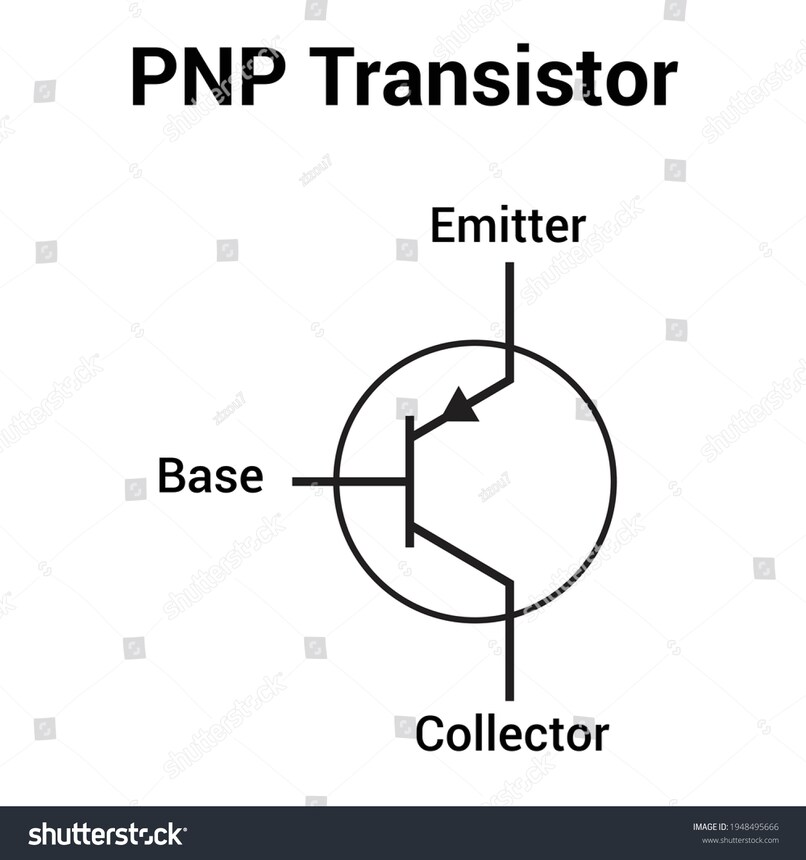
Working Of The PNP Transistor
Three terminals make up a PNP transistor: the Collector (C), Emitter (E), and Base (B). When two PN junction diodes are connected back to back, the PNP transistor functions like that. The negative terminal of a voltage source (VEB) is linked to the Base terminal (N-type), while the positive terminal is connected to the Emitter(P-type). The Emitter-Base connection is therefore wired in forward bias. Additionally, a voltage source's positive terminal (VCB) is coupled with the N-type base terminal, while the negative terminal is coupled with the collector terminal (P-type). Consequently, reverse bias is applied to the Collector-Base junction. The depletion region at the emitter-base junction is constrained due to this sort of bias because it is coupled in the direction of forward bias. The depletion region at the Collector-Base junction is wide because of the reverse bias at the Collector-Base junction.
NPN Transistor In Detail
A P-type semiconductor is sandwiched between two N-type semiconductors to create an NPN transistor, which is the most popular type of bipolar junction transistor. The NPN transistor's symbol is depicted in the figure below. The arrowhead depicts the collector current (IC), base current (IB), and emitter current (IE) in their typical directions.
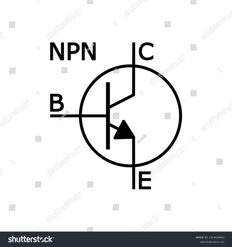
Working Of NPN Transistor
There are two junctions and three terminals in an NPN transistor. In a forward bias condition, supply voltage (VEE) connects the base-emitter junction. Additionally, supply voltage (VCC) connects the collector-base junction when it is in a reverse bias condition. The N-type semiconductor's negative supply source terminal (VEE) is connected in the forward bias condition (Emitter). Similarly, in a reverse bias condition, the N-type semiconductor is linked to the positive terminal of the supply source (VCC) (Collector). Electrons make up the majority of the charge carriers in N-type emitters. As a result, electrons begin to flow from an N-type emitter to a P-type base, where they continue to flow. A P-type semiconductor makes up the base. Base current ( IB) is the current that flows through the circuit as a result of the recombination.
Frequently Asked Questions (FAQs)
The very fundamental operation of a transistor is to regulate the strength of a very little current passing through a second channel to control the flow of current through one channel.
Plots that can show the relationship between a transistor's current and voltage in a specific arrangement are called transistor characteristics.
Input characteristics: By keeping the output voltage constant, it will provide information on how the input current changes when the input voltage varies.
Output characteristics: By maintaining a constant input current, this plot compares the output current to the output voltage.
Characteristics of the current transfer: By maintaining a constant voltage, this plot illustrates how the output current varies with the input current.
smaller and less expensive.
less sensitive mechanically.
functioning at a low voltage.
extraordinary longevity.
No energy is used.
switching quickly.
Circuits with higher efficiency can be created.
Higher electron mobility is absent from transistors.
As a result of electrical and thermal events, transistors are readily destroyed. Consider treating electrostatic discharge as an example.
Radiation and cosmic rays have an impact on transistors.
Also Read
11 Jan'25 05:47 PM
25 Nov'24 06:23 PM
20 Nov'24 02:59 PM
20 Nov'24 10:57 AM
15 Nov'24 01:49 PM
12 Nov'24 11:20 PM
12 Nov'24 10:24 PM
12 Nov'24 09:39 PM