Classification of solids on the basis of Band theory
Solids can be classified into different categories based on their electrical conductivity, which is fundamentally explained by the Band Theory. Band Theory describes the quantum states of electrons in a solid, where energy levels form bands – the valence band and the conduction band. The nature of these bands and the gap between them determine whether a solid behaves as a conductor, insulator, or semiconductor. Understanding this classification helps in the development of various electronic devices and materials with specific properties for technological applications. In this article, we will explore how solids are categorized based on their band structures and the implications of these classifications. Also, we will see some of the solved examples based on this concept.

On the Basis of Conductivity
Based on the relative values of electrical conductivity $(\sigma)$ or resistivity, the solids are broadly classified as:
Conductor: The materials which easily allow the flow of electric current through them are called conductors. Metals such as copper, silver, iron, aluminium, etc. are good conductors of electricity. They possess very low resistivity (or high conductivity).
$\begin{aligned} & \text { i.e } \rho \sim 10^{-2}-10^{-8} \Omega m \\ & \sigma \sim 10^2-10^8 S m^{-1}\end{aligned}$
Insulator: The materials which do not allow the flow of electric current through them are called insulators. Insulators are also called poor conductors of electricity. Rubber, wood, diamond, and plastic are some examples of insulators. They have high resistivity (or low conductivity).
$\begin{aligned} & \text { i.e } \rho \sim 10^{11}-10^{19} \Omega \mathrm{m} \\ & \sigma \sim 10^{-11}-10^{-19} \mathrm{Sm}^{-1}\end{aligned}$
Semiconductors: They have resistivity or conductivity intermediate to metals and insulators.
$\begin{aligned} & \text { i.e } \rho \sim 10^{-5}-10^6 \Omega \mathrm{m} \\ & \sigma \sim 10^5-10^{-6} \mathrm{Sm}^{-1}\end{aligned}$
Note- At 0 K, it behaves like an insulator (Si, Ge)
Semiconductors are Further Divided as Follows:
(i) Elemental semiconductors: These are semiconductors composed of a single element. Examples include Silicon (Si) and Germanium (Ge).
(ii) Compound semiconductors: These are semiconductors composed of two or more elements. Examples include:
- Inorganic: Cadmium Sulfide (CdS), Gallium Arsenide (GaAs), Cadmium Selenide (CdSe), Indium Phosphide (InP), etc.
- Organic: Anthracene, doped Phthalocyanines, etc.
- Organic polymers: Polypyrrole, Polyaniline, Polythiophene, etc.
Materials are also classified based on energy bands. To understand this classification, it's essential to first know about the concept of energy bands.
Energy Band Theory
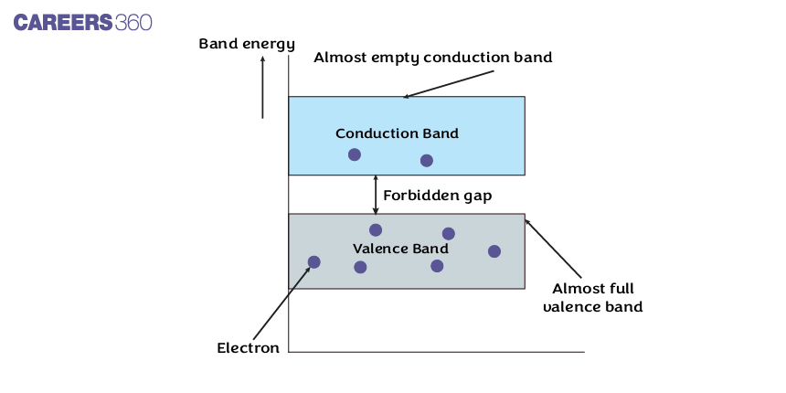
There is a number of energy bands in solids but three of them are very important which are shown in the below figure.

What is a Valence Band?
The energy band which is formed by grouping the range of energy levels of the valence electrons or outermost orbit electrons is called a valence band. The valence band is present below the conduction band as shown in the above figure.
So Electrons in the valence band have lower energy than the electrons in the conduction band. The electrons present in the valence band are loosely bound to the nucleus of an atom.
What is a Conduction Band?
The energy band which is formed by grouping the range of energy levels of the free electrons is called a conduction band. Generally, the conduction band is empty but when external energy is applied the electrons in the valence band then electrons jump into the conduction band and become free electrons.
Electrons in the conduction band have higher energy than the electrons in the valence band. The conduction band electrons are not bound to the nucleus of the atom.
What is the Forbidden Band or Forbidden Gap?
The energy band which is present between the valence band and conduction band by separating these two energy bands is called a forbidden band. In solids, electrons cannot stay in a forbidden band because there is no allowed energy state in this region.
The energy associated with the forbidden band is called the energy gap and it is measured in unit electron volt (eV). The applied external energy in the form of heat or light must be equal to the forbidden gap in order to push an electron from the valence band to the conduction band.
Classification of Materials Based on a Forbidden Gap
Conductors
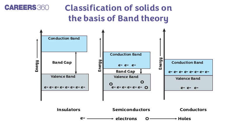
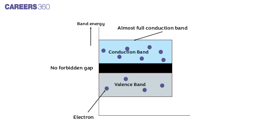
In a conductor, the valence band and conduction band overlap each other as shown in the below figure. Therefore, there is no forbidden gap in a conductor.

A small amount of applied external energy provides enough energy for the valence band electrons to move into the conduction band. When valence band electrons move to the conduction band they become free electrons.
In conductors, a large number of electrons are present in the conduction band at room temperature and these electrons move freely by carrying the electric current from one point to another.
Insulators
The forbidden gap between the valence band and conduction band is very large in insulators as shown in the below figure.
Note- When the energy gap between the valence band and conduction band is more than 3 eV. then the material is an insulator.

Normally, in insulators, the valence band is fully occupied with electrons due to the sharing of outermost orbit electrons with the neighbouring atoms. At the same time, no electrons are present in the conduction band. Free electron density is negligible in the case of the insulator. The electrons in the valence band cannot move by themself because they are locked up between the atoms.
Semiconductors
In semiconductors, the forbidden gap between the valence band and conduction band is very small as shown in the below figure.
Note- When the Energy gap between the valence band and conduction band is less than 3 e.v. Then the material is a semiconductor.

At low temperatures, the valence band is completely occupied with electrons and the conduction band is empty because the electrons in the valence band do not have enough energy to move into the conduction band. Therefore, the semiconductor behaves as an insulator at low temperatures.
However, at room temperature, some of the electrons in the valence band gain enough energy in the form of heat and move into the conduction band. When the temperature increases, then the number of valence band electrons moving into the conduction band also increases. So free electron density in the conduction band increases. This shows that the electrical conductivity of the semiconductor increases with an increase in temperature.
Learn Classification of Solids on the Basis of Band Theory With the Given Video Below
Solved Examples Based on Classification of Solids on the Basis of Band Theory
Example 1: Carbon, silicon and germanium have four valence electrons each. At room temperature, which one of the following statements is most appropriate?
1) The number of free electrons for conduction is significant only in Si and Ge but small in C.
2) The number of free conduction electrons is significant in C but small in Si and Ge.
3) The number of free conduction electrons is negligibly small in all three.
4) The number of free electrons for conduction is significant in all three.
Solution:
Since carbon is non-metal while silicon and germanium are semiconductors,hence at room temperature, free electrons for conduction are significant for Si and Ge but negligible in carbon.
Hence, the answer is the option (1).
Example 2: At absolute zero, Si acts as:
1) non-metal
2) metal
3) insulator
4) none of these
Solution:
Any semiconductor behaves like an insulator at 0 K.
So, at 0K, Si also behaves as an insulator.
Hence, the answer is the option (3).
Example 3: The manifestation of band structure in solids is due to
1) Heisenberg’s uncertainty principle
2) Pauli’s exclusion principle
3) Bohr’s correspondence principle
4) Boltzmann’s law
Solution:
It is due to Pauli's exclusion principle: no two electrons can have the same set of all four quantum numbers. Hence electrons occupy gradually higher energy levels.
Hence, the answer is the option (2).
Example 4: A solid which is transparent to visible light and whose conductivity increases with temperature is formed by
1) metallic bonding
2) ionic bonding
3) covalent bonding
4) van der Waals bonding
Solution:
The energy gap between the valence band and conduction band is less than 3 e.v.
wherein
1) $\Delta E_{g \text { lies between conductor } \& \text { insulator }}$
2) Both electrons and holes are responsible for conductivity.
3) At 0 K behave like an insulator ( $\mathrm{Si}, \mathrm{Ge}$ )
This property corresponds to semiconductors. The bonds formed by semiconductors are covalent.
Hence, the answer is the option (3).
Example 5: A p.n. junction diode is operated in forward biasing mode at 300K temperature. The voltage (in mV) at which the forward bias current equals the reverse saturation current would be:(Take, Boltzmann's constant (k)$=8.62 \times 10^{-5} \frac{\mathrm{eV}}{\mathrm{K}}$, $\left.\log _e 2=0.693\right)$)
1) 17.92
2) 1.792
3) 179.2
4) 0.179
Solution:
We know forward biasing current in a p.n diode is given by
$
I=I_0\left(e^{\frac{\varepsilon V}{K T}}-1\right)
$
When $I=I_0, I_0=I_0\left(e^{\frac{\varepsilon V}{K T}}-1\right)$
$
\Rightarrow 2=e^{\frac{i V}{K T}}
$
Taking natural logs on both sides
$
\begin{aligned}
& \Rightarrow \log _c 2=\frac{e V}{K T} \\
& \begin{aligned}
\Rightarrow V & =\frac{K T}{e} \log _e 2 \\
& =\frac{8.62 \times 10^{-5}\left(\frac{e V}{K}\right) \times 300 \mathrm{~K}}{e} \times 0.693 \\
& =17.92 \times 10^{-3} V \\
& =17.92 \mathrm{mV}
\end{aligned}
\end{aligned}
$
Hence, the answer is the option (1).
Summary
Solids are classified based on their electrical properties using a theory that is known as band theory. When combined in the solid state, atoms have their outermost electrons arranged into bands that contain specific energy levels. For example, the most important bands include the valence band which contains electrons and the conduction band which is higher in energy and often not filled with any electron. This space between these bands is referred to as band gap, and it dictates how solids behave.
