Difference Between Zener Breakdown and Avalanche Breakdown
In this article we will understand in detail about zener breakdown and avalanche breakdown, what is the breakdown voltage of zener diodes? How does the avalanche breakdown in a diode occur when we apply the reverse voltage? What is zener breakdown? What is avalanche breakdown? And the difference between zener breakdown and avalanche breakdown. Breakdown means interruption or collapse in the system.
This Story also Contains
- What Is Avalanche Breakdown and Explain
- What Is Zener Breakdown and Explain
- Zener Breakdown and Avalanche Breakdown Difference:
- Important Related Topics
What Is Avalanche Breakdown and Explain
Avalanche breakdown definition: It is an occurrence that happens when the high reverse voltage is applied across the lightly doped P-N junction diode.
Now let us understand how the avalanche breakdown in a diode occurs when we apply the reverse voltage.
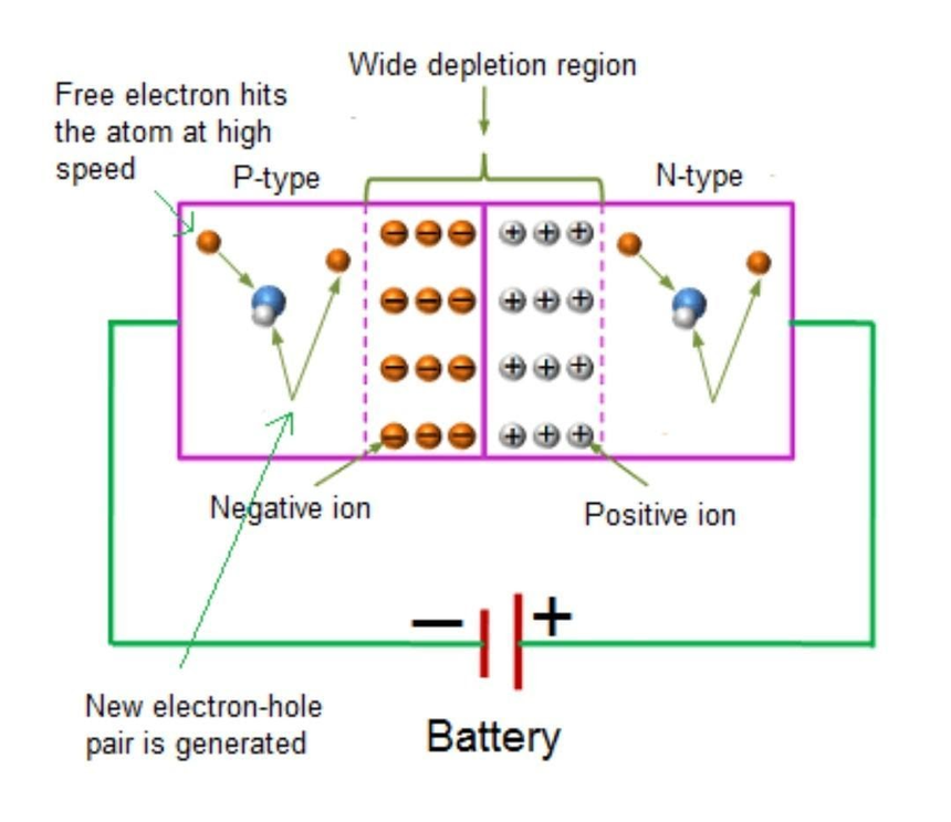
Now we know that in reverse bias conditions, the electric current that we are getting is due to the minority charge carriers. So in the reverse bias, as we intensify the applied reverse voltage, the thickness of the depletion region will intensify, and, due to that the immobile ions in this depletion region will also increase. So because of the inclination of the immobile ions, the electric field in the depletion region will become stronger and due to this stronger electric field, the minority charge carriers which are in the surrounding area to this depletion region will get accelerated.
But after the applied voltage stretches to the breakdown voltage of the silicon diode then the kinetic energy that is extended by these charge carriers will knock off the bound of the silicon atom. In the case of crystal level, accelerated electrons may collide with the silicon atom and when it has enough kinetic energy then it can knock out a bound charge or the valence charge of this atom. Now we have two free electrons under the influence of the Electric field. Now these two electrons can collide with the two more atoms and they can knock out the two more electrons.
Similarly, now these four electrons will again collide with the four more atoms and they can knock out the four more electrons. Thus due to this collision, the number of free charge carriers in the depletion region will intensify significantly. And because of this intensification in these charge carriers, we will see an abrupt hype in the reverse saturation current. So this effect is known as the Avalanche breakdown effect and the voltage after which it occurs is known as the Avalanche breakdown voltage.
We have seen this Avalanche breakdown is due to the impact ionization, meaning that the high energy charged particles can knock out the bound electrons from the silicon atom, and in this way, it creates the electron-hole pair. So for the normal diode, this region of operation should be avoided because when the applied voltage is more than this breakdown voltage then the diode starts conduct, citing in the reflection-holen also. Moreover, if there is no current limiting resistor in series with this diode then due to the very large current or very high power dissipation this diode may get damaged.
So for the normal diode, this region of operation should be avoided but some diodes are meant to be used in this breakdown region and this diode is known as the zener diode. But in Zener diodes, the breakdown, mechanism is different from the avalanche effect in diodes. So now let us understand what exactly the zener breakdown mechanism is.
What Is Zener Breakdown and Explain
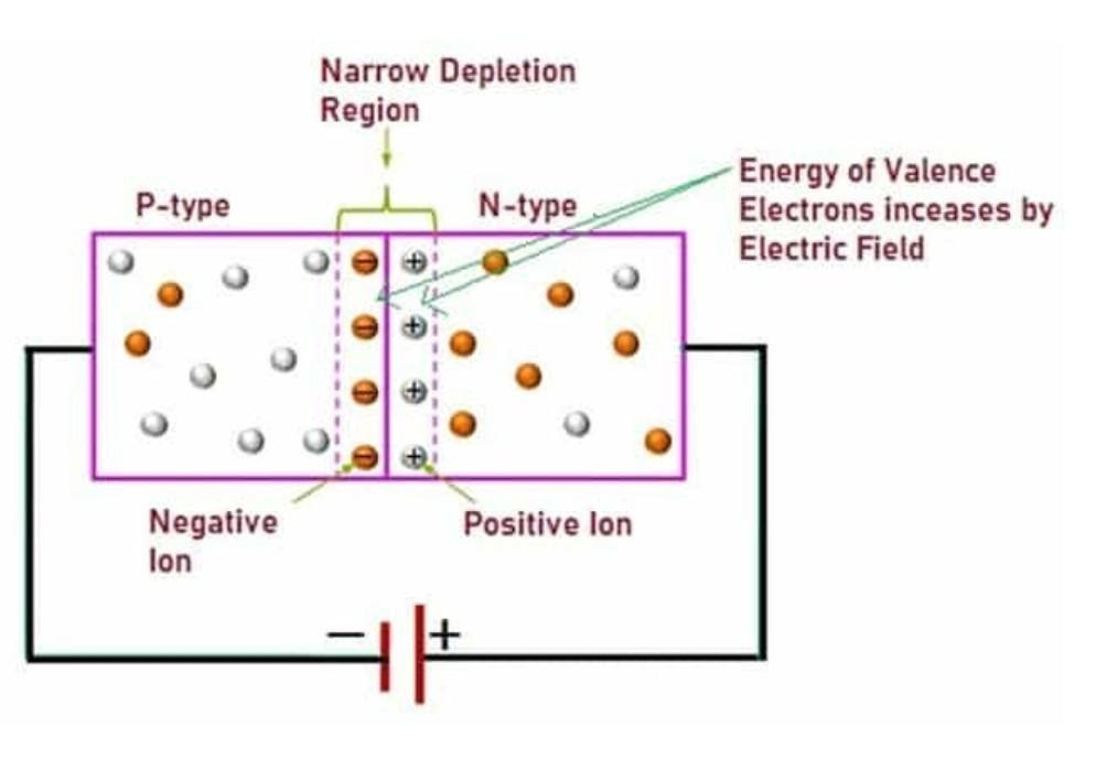
Zener breakdown definition: It is an occurrence that happens when a low reverse voltage is applied in a heavily doped P-N junction diode.
The P and N type regions of the Zener diode are heavily doped meaning that the number of impurity atoms in these p and n regions will be more due to the number of free charge carriers in both regions will be more. So due to this heavy doping the width of the depletion region will be much narrower compared to the normal diode because now when the electron diffuses from the n side to the p side then it will get recombined very much near to the junction itself. In addition to that, due to this heavy doping, this small depletion area will have a greater number of immovable ions matched to the normal diode.
So due to this the built-in electric field inside this depletion region will be much stronger and when this diode is in reverse bias then the external electric field will also get added with this built-in electric field and due to that the electric field in this depletion region will become very strong. And at one particular voltage, it will become so strong that it can knock out the bound electrons of these silicon atoms. So due to this very strong electric field, many charge carriers are generated and because of the very narrow depletion region they can tunnel through it and they can reach the other side of the depletion region.
So because of the very high electric field, many charge carriers are produced in this depletion region and current starts flowing rapidly in the reverse direction. This effect is called the zener breakdown effect and the voltage beyond which it takes place is called the zener breakdown Voltage. However, the zener effect is seen at the lower breakdown voltages.
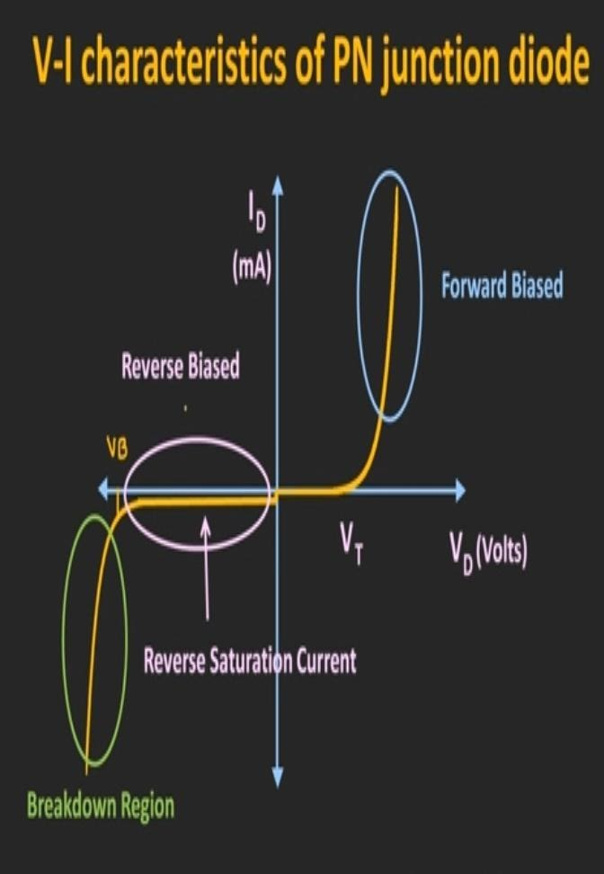
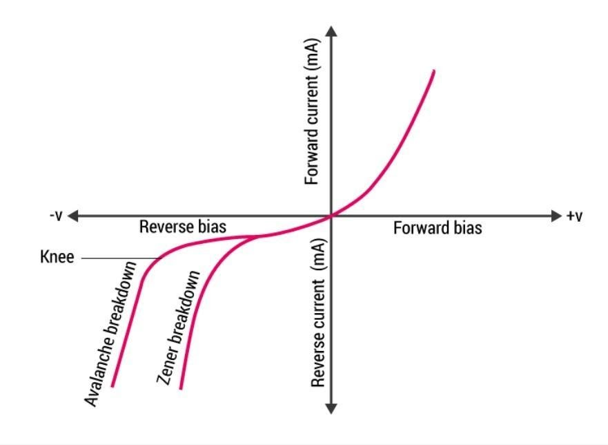
From the graph, we observe that even if we increase the applied Voltage beyond the zener voltage then the Voltage across the diode will almost remain constant. And only the current through the diode will increase. , So because of this property, the zener diode is used as a voltage regulator in many appliances.
Till now we have studied zener and avalanche breakdown. Now let us understand the difference between avalanche and zener breakdown.
Also Read:
Zener Breakdown and Avalanche Breakdown Difference:
The difference between avalanche breakdown and zener breakdown is given below:
- Difference based on doping of diode:
Avalanche breakdown in a semiconductor diode occurs when the diodes are lightly doped whereas zener breakdown occurs when the diode is heavily doped. - Difference based on the process:
The avalanche breakdown effect occurs due to the impact ionization whereas the Zener breakdown effect occurs due to the strong electric field (quantum tunneling). - Difference based on the voltages:
The avalanche breakdown effect is seen at higher breakdown voltages (typically, higher than 6V) whereas the Zener breakdown effect is seen at lower breakdown voltages (typically, less than 4V). - Difference based on temperature coefficient:
When the avalanche breakdown effect is predominant, the temperature of breakdown voltage is positive, meaning that as the temperature increases the breakdown voltage will increase whereas if the zener breakdown effect is predominant then the temperature coefficient of breakdown voltage is negative, meaning that as the temperature increases the breakdown voltage will reduce.
|
Related Topics link, |
Important Related Topics
Forward Bias P-N Junction
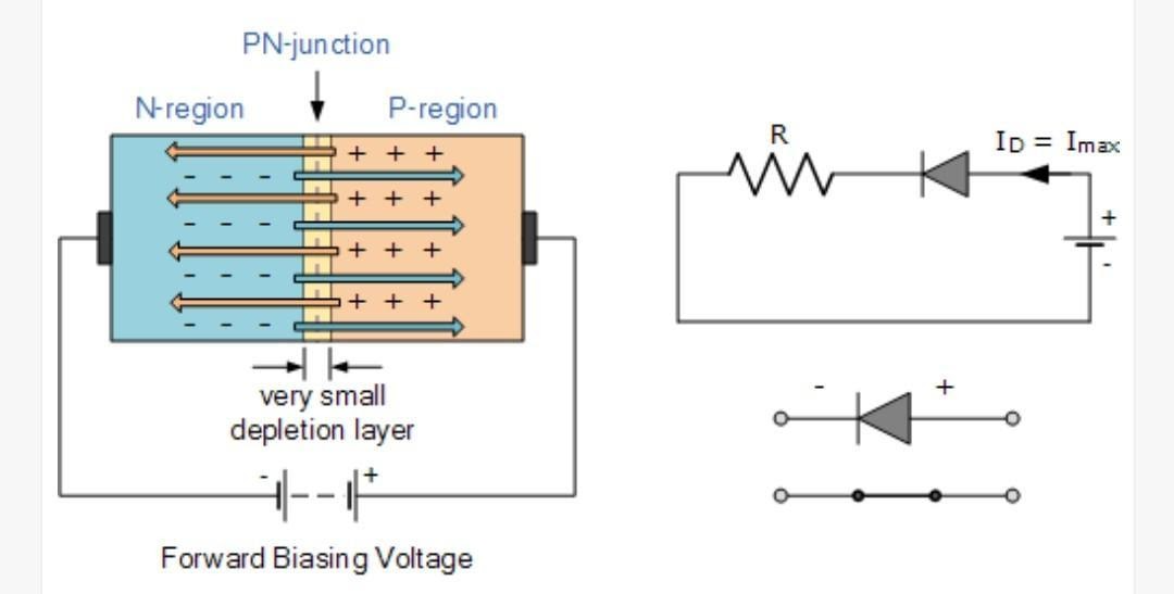
In the case of forward bias, the positive station of the series is connected to the P side and the negative station of the series is connected to the N side. In this forward bias condition, the external electric field is in the opposite direction to the built-in electric field, and due to that the affected electric field at the junction will reduce. So in the forward condition, the electron in the n-type region and the holes in the p-type region will get pushed toward the junction. So because of that the thickness of the depletion region will lessen. So the operational resistance that is accessible by the depletion region will also decrease. When the functional voltage is more than the barrier potential of this PN junction then the resistance occupied by the depletion region is insignificant. As we increase the externally applied biasing, the voltage in the circuit will increase.
Reverse Bias P-N Junction
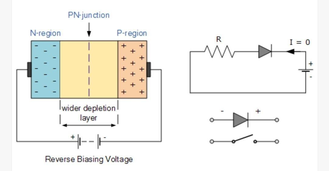
In the reverse bias condition, the negative station of the series is connected to the P side and the positive station of the series is connected to the N side. So in this condition, the electrons which are mainstream carriers in this N-type region will get engrossed toward the positive terminal of the battery and similarly, the holes on the P-side region will get engrossed toward the negative terminal of the battery. And because of that other ions will get generated near the junction. So we can say that the thickness of the depletion region will intensify.
So in the reverse bias condition, as we increase the reverse bias voltage the thickness of the depletion region will additionally intensify. Due to that virtually, there is no flow of current due to the majority of carriers. But in the case due to the built-in electric field, minority carriers in both regions will be able to cross this depletion region. However, the minority carriers are very less in comparison to the majority carriers. So the flow of current that exists in this reverse bias condition is known as reverse saturation current. The reverse saturation current does not change much even if we increase the reverse bias voltage but there is a limit to the maximum reverse voltage that can be applied to this PN junction.
So, if we continuously increase this reverse voltage then we will reach a point which is known as the breakdown voltage of the diode. After the breakdown voltage for the diode, a lot of minority carriers will be seen at the depletion region and unexpectedly the diode behaves very profoundly. This effect is known as the Avalanche effect in diodes. Now let us study in detail about zener and avalanche breakdown.
Frequently Asked Questions (FAQs)
The temperature coefficient of avalanche breakdown voltage is positive whereas the temperature coefficient of zener breakdown voltage is negative.
The breakdown voltage of avalanche breakdown is higher than 6V.
Because in reverse biasing the potential at the junction increases.
Breakdown voltage of the zener diode is less than 4V.
Avalanche means the sudden occurrence or fall of something.