

Extrinsic Semiconductors - Definition, Types, FAQs
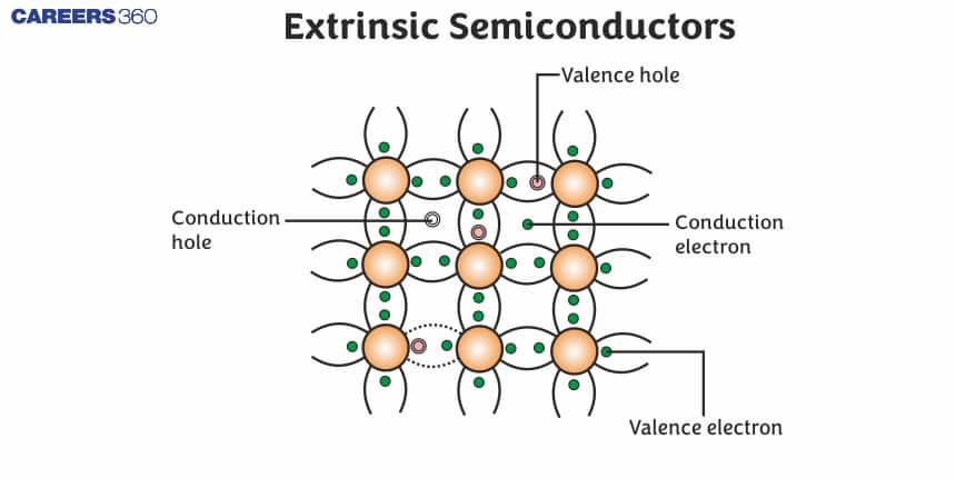
In an intrinsic semiconductor, conductivity is very low since it contains only pure material like silicon or germanium without any impurities added. Such semiconductors are of no use in the manufacture of most electronic devices. A small quantity of impurity is added to such semiconductors to increase their conductivity. The process by which impurities are added is called doping, and the semiconductor thus obtained is called an extrinsic semiconductor.
Thus, by the addition of impurities, the number of free charge carriers in a semiconductor increases, thereby increasing its conductivity and making it useful in practical applications. There are two major types of extrinsic semiconductors: n-type and p-type, depending upon the type of impurity added to the semiconductor. In this article, we will learn about what extrinsic semiconductors are, their types, applications, and how different they are from intrinsic semiconductors.
This Story also Contains
- What is a Semiconductor?
- What is Extrinsic Semiconductor?
- Types of Extrinsic Semiconductors
- N-type Semiconductor
- P-type Semiconductor
- Factors Affecting Extrinsic Semiconductors
- Applications of Extrinsic Semiconductor
- Energy Band Diagram For P-type and N-type Semiconductor
- Difference Between P-type and N-type Semiconductors
What is a Semiconductor?
A semiconductor is a material whose ability to conduct electricity lies between that of a conductor (like copper) and an insulator (like rubber). In simple words, it conducts electricity partly, depending on temperature, light, or impurities added to it.
At low temperatures, semiconductors act like insulators, but as temperature increases, their conductivity also increases. This property makes them very useful in electronic devices. Common examples of semiconductors are silicon (Si) and germanium (Ge).
Types of Semiconductors
- Intrinsic semiconductor
- Extrinsic semiconductor
What do you mean by doping?
Doping is known as the controlled mixing of impurities in semiconductors. The impurities are called dopants.
What is Extrinsic Semiconductor?
Extrinsic semiconductor definition: Extrinsic semiconductor is a special kind of semiconductor that drastically increases the electric conductivity of the semiconductor by mixing impurities in a controlled manner. When the conductivity of a semiconductor gets increased by doping, then the semiconductor is called an extrinsic semiconductor.
If we define impurity, impurities meaning in a semiconductor is not the constituent particle of the semiconductor, it means other substances like arsenic, phosphorus, etc.
Extrinsic semiconductor examples: Germanium (Ge) and silicon (Si) doped with arsenic (As), phosphorus (P), etc.
Types of Extrinsic Semiconductors
Extrinsic semiconductors are classified into two types depending on the doping and the majority charge carriers.
- n-type semiconductor
- p-type semiconductor
N-type Semiconductor
If pentavalent impurities or elements are dropped as impurities in the crystal of an intrinsic semiconductor in a controlled manner, the crystal thus formed is called an n-type semiconductor or n-type extrinsic semiconductor.
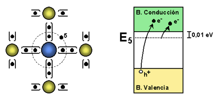
Pentavalent impurities are called donors as they have five electrons in the outermost shell.
Examples of n-type semiconductors
Arsenic (As), and phosphorus (P) act as an n-type semiconductor in pure silicon (Si) or germanium (Ge).
P-type Semiconductor
If trivalent impurities or elements are doped as impurities in a crystal in an intrinsic semiconductor in a controlled manner, the crystal thus formed is called a p-type semiconductor or p-type extrinsic semiconductor.
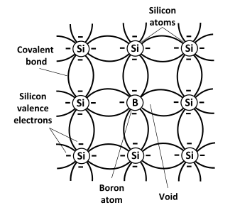
Trivalent impurities examples/ Examples of p-type semiconductors
Boron (Br), aluminum (Al) doped in pure silicon (Si), or germanium (Ge) which works as a p-type semiconductor.
Factors Affecting Extrinsic Semiconductors
- Doping Element type
- Amount of impurities added
- Temperature
- Energy band gap
- Mobility of charge carriers
- Type of semiconductor material
Applications of Extrinsic Semiconductor
- Diodes (P-N junction diode, Zener diode, LED)
- Transistors
- Photodiodes
- Solar cells
- Lasers
- Phototransistors
- Rectifiers
- Light detectors
Energy Band Diagram For P-type and N-type Semiconductor
P-type Semiconductor Diagram

N-type Semiconductor Diagram

Difference Between P-type and N-type Semiconductors
| n-type Semiconductor | p-type Semiconductor |
| Pentavalent impurities | Trivalent impurities |
| Electrons are the majority of charge carriers | Holes are the majority of charge carriers |
| Holes are the minority charge carriers | Electrons are the minority charge carriers |
| Donor impurities that donate free electrons. | Acceptor impurities that create holes. |
| Conductivity is due to the movement of electrons. | Conductivity is due to the movement of holes. |
| Donor energy levels are close to the conduction band. | Acceptor energy levels are close to the valence band. |
| Used in transistors, diodes, and other electronic devices. | Used in LEDs, photodiodes, and other electronic devices. |
| Silicon is doped with phosphorus or arsenic. | Silicon doped with boron or gallium. |
Also read:
Frequently Asked Questions (FAQs)
The substances having electrical conductivity intermediate between conductors and insulators are called semiconductors.
The release of an electron creates a position known as hole , which is opposite in charge of an electron.
The separation between two consecutive energy levels in a solid is known as a forbidden band.
The energy band that is formed by energy levels in which the electrons of a substance can reside, is called valence band.
The energy levels possessed by the free electrons or conduction electrons of a substance constitute the band which is known as conduction band.
When germanium doped with indium, p-type semiconductor is obtained.
A semiconductor has generally valence electrons of 4.
