

Intrinsic Semiconductors - Undoped Semiconductors, Definition, Working Mechanism, FAQs
The intrinsic semiconductors are the semiconductors that have no impurity in them. They are the purest form of semiconductors. They have no other element, such as doping, in them. There are the two types of semiconductors. In this article, we will discuss what intrinsic semiconductors are, the intrinsic semiconductor diagram for energy bands, the working mechanism of intrinsic semiconductors, examples of intrinsic semiconductors, the Fermi energy level and carrier concentration formula of intrinsic semiconductors, and intrinsic semiconductor current.
This Story also Contains
- What are intrinsic semiconductors?
- Example of Intrinsic Semiconductor
- Working Mechanism of Intrinsic Semiconductors
- Fermi Energy Level Of Intrinsic Semiconductor
- Energy Band diagram for Intrinsic Semiconductor
- Intrinsic Carrier Concentration
- Intrinsic Semiconductor Current
What are intrinsic semiconductors?
Intrinsic semiconductors are chemically pure semiconductors that are free of impurities. The intrinsic semiconductor behaves as an insulator at absolute zero temperature because all electrons are participating in covalent bonding. So, there are no free electrons. When temperature is provided to the material, the covalent bonds break down and a pair of electrons and holes are generated. These free electrons and holes lead the material to behave as a semiconductor. In an intrinsic semiconductor, the number of free electrons is equal to the number of holes, i.e., $n_e=n_h=n_i$. Another name for intrinsic semiconductors is undoped semiconductors or i-type semiconductors. So, we can say that a semiconductor in its purest form is called an intrinsic semiconductor.
Example of Intrinsic Semiconductor
- Silicon: It is widely used in the production of electronics like diodes, transistors, and solar cells. Its band gap energy is 1.1 eV.
- Germanium: It is used in high-speed transistors and infrared detectors. Germanium is sensitive to temperature variations, as the band gap energy is only 0.66 eV.
Working Mechanism of Intrinsic Semiconductors
Take, for example, a Si intrinsic semiconductor or Ge intrinsic semiconductor
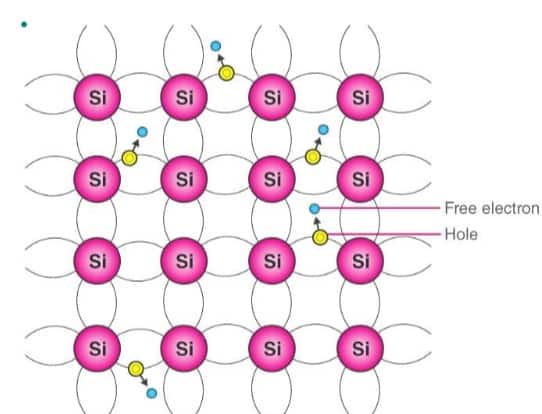
Both elements have four electrons in their outermost shell, or valence shell, as seen in their electron configurations. The electrons gather more thermal energy and consequently break away from their shell as the temperature of the semiconductor rises. The atoms in the crystal lattice are ionized, which causes a vacancy in the link between them. There is a hole in the position where the electron is dislodged, which is comparable to an effective positive charge. The hole is subsequently filled by a free electron, turning the previous vacant position into a hole and the former unoccupied position into a neutral position. The hole, or effective positive charge, is transferred from one place to another in this manner.
The number of free electrons in an intrinsic semiconductor is equal to the number of holes. So, $n_e=n_h=n_i$
The number of total intrinsic carrier concentration, which is equivalent to the total number of holes or electrons, is given by $n_i$.
When an intrinsic semiconductor's temperature is T=0 K, it behaves like an insulator. The electrons become excited and travel from the valence band to the conduction band when the temperature rises ($\mathrm{T}>0$).These electrons partially fill the conduction band, leaving an equivalent number of holes in the valence band.
Fermi Energy Level Of Intrinsic Semiconductor
The Fermi level is that energy level where the probability of finding an electron is 0.5 (50%) at absolute zero temperature, i.e., at T = 0 K (-273 ${ }^{\circ} \mathrm{C}$). The Fermi level is considered the highest energy state that can be occupied. The number of holes in the valence band in an intrinsic semiconductor is equal to the number of electrons in the conduction band. As a result, the probability of occupying energy levels in the valence and conduction bands is the same. So the middle of the forbidden energy band is the Fermi level in an intrinsic semiconductor.
Energy Band diagram for Intrinsic Semiconductor
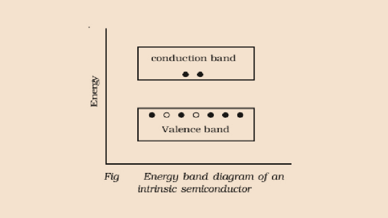
First, the conduction band was empty in the above energy band diagram, whereas the valence band was filled. Some heat energy can be delivered to it once the temperature has been raised. As a result of exiting the valence band, electrons from the valence band are supplied to the conduction band. The flow of electrons will be random as they move from the valence to the conduction band. The crystal's holes can also flow freely in any direction.
As a result, the TCR (temperature coefficient of resistance) of this semiconductor will be negative. The TCR indicates that when the temperature rises, the material's resistance decreases, and the conductivity of the intrinsic semiconductor rises. This shows the effect of temperature on the conductivity of intrinsic semiconductors.
Related Topics, |
Intrinsic Carrier Concentration
Two types of charge carriers are formed in intrinsic semiconductors when the valence electrons break the covalent bond and leap into the conduction band. Free electrons and holes are what they are. Carrier concentration in intrinsic semiconductors refers to the number of electrons per unit volume in the conduction band or the number of holes per unit volume in the valence band.
Electron-carrier concentration refers to the number of electrons per unit volume in the conduction band, while hole-carrier concentration refers to the number of holes per unit volume in the valence band. The number of electrons created in the conduction band in an intrinsic semiconductor is equal to the number of holes generated in the valence band.
As a result, the concentration of electron carriers is equal to the concentration of hole carriers. It can be written as,
$$
n=p=n_i
$$
Where,
- n = electron-carrier concentration
- P = hole-carrier concentration
- $n_i$ = intrinsic carrier concentration
Intrinsic Carrier Concentration Formula
In the valence band, hole concentration is expressed as
 $$
$$
\mathbf{p}=\mathbf{N}_{\mathrm{v}} \ \mathrm{e}^{\frac{-\left(\mathbf{E}_{\mathrm{f}}-\mathbf{E}_{\mathrm{v}}\right)}{\mathrm{K}_{\mathrm{b}} \mathbf{T}}}
$$
In the conduction band, electron concentration is expressed as
$$
\mathbf{n}=N_c \ e^{\frac{-\left(E_c-E_f\right)}{K_b T}}
$$
where, $K_B$ is the Boltzmann constant
$T$ = Absolute temperature of a pure semiconductor
$\mathrm{N}_{\mathrm{c}}$ = effective density of states in conduction band
$\mathrm{N}_{\mathrm{v}}$ = effective density of states in valence band
Intrinsic Semiconductor Current
Electric current flows due to both electron and hole movements in intrinsic semiconductors, i.e., electrons in the conduction band that have been released from their lattice locations can travel through the material. Other electrons can also jump between lattice positions to fill the voids created by the released electrons. The holes seem to migrate in the opposite direction of the free electrons across the material; this extra mechanism is known as hole conduction. The density of energy levels determines the electron density in the conduction band, which affects current flow in an intrinsic semiconductor. This current is extremely temperature-sensitive.
Condition of Intrinsic Semiconductor at Room Temperature
At room temperature, an intrinsic semiconductor has a few free electrons and holes. So, there is a flow of current, but this current is low. While an intrinsic or pure semiconductor behaves like an insulator at absolute zero temperature because all electrons are participating in covalent bonding. So, there are no free electrons to participate in charge transfer. When thermal energy is provided to the material, the covalent bonds break down and a pair of electrons and holes is generated. These free electrons and holes lead the material to behave as a semiconductor. The conductivity of an intrinsic semiconductor decreases with a decrease in temperature, so it behaves as an insulator at absolute zero temperature (0 Kelvin).
Doping
The addition of impurities to a semiconductor is known as doping. During the preparation of an extrinsic semiconductor, the amount of impurity injected into the material must be controlled. A semiconductor can have one impurity atom added to every 108 atoms. The number of holes or electrons can be increased by introducing the impurity to improve its conductivity. If a pentavalent impurity with 5 valence electrons is added to a pure semiconductor, then it will be a p-type extrinsic semiconductor, while if a trivalent impurity is added to a pure semiconductor, then it will be an n-type semiconductor. On this basis, extrinsic semiconductors are categorized into two types: n-type and p-type semiconductors.
Also read:
Frequently Asked Questions (FAQs)
The electron is responsible for the flow of current during the forward bias, while the hole is responsible for the flow of current during the reverse bias process.
A hole represents the absence of an electron in any semiconductor.
The intrinsic semiconductors are used in making transistors.
The energy difference between the topmost of the valence band and the lowest of the conduction band is known as the energy band gap for any semiconductor.
Intrinsic semiconductors exhibit low conductivity at room temperature, as there are no impurities in these semiconductors.
The intrinsic type of semiconductor is pure, whereas the extrinsic type is one that can have impurities introduced to make it conductive.
Silicon and germanium are the two elements.
The intrinsic conductivity of a semiconductor is defined as the concentration of impurities and structural flaws in the semiconductor.
Electrons and holes are employed in this experiment.
Intrinsic semiconductors are made of the purest semiconductor material.
