P N Junction - Meaning, Formation, Applications, FAQs
What is PN junction diode?
Junction meaning: A pn junction is defined as a boundary between the two type of semiconductor materials which are p-type and n-type in a single crystal of semiconductor. P-type semiconductors are those semiconductors which are formed by the doping of trivalent element and has holes as the majority charge carriers. N-type semiconductors are those semiconductors which are formed by the doping of pentavalent elements and has electrons as the majority charge carriers.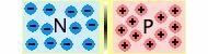
JEE Main 2025: Physics Formula | Study Materials | High Scoring Topics | Preparation Guide
JEE Main 2025: Syllabus | Sample Papers | Mock Tests | PYQs | Study Plan 100 Days
NEET 2025: Syllabus | High Scoring Topics | PYQs
Formation of PN junction
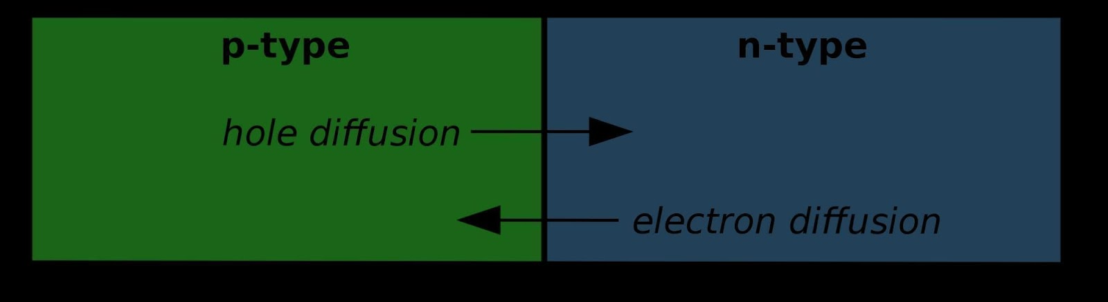
When n-type and p-type semiconductors are joined to form a pn diode junction, there are several processes which occur in it.
We know that the concentration of electrons is high in n-type semiconductors as compared to p-type semiconductors and the concentration of holes is high in p-type semiconductors as compared to n-type semiconductors.
Also read :
- NCERT notes Class 12 Physics Chapter 14 Semiconductor Electronics: Materials, Devices and Simple Circuits
- NCERT solutions for Class 12 Physics Chapter 14 Semiconductor Electronics: Materials, Devices and Simple Circuits
- NCERT Exemplar Class 11 Physics Solutions Chapter 14 Semiconductor Electronics: Materials, Devices and Simple Circuits
When an electron diffuses from n to p, it leaves behind an ionized immobile positive ion which get accumulated at the n-side of the junction. Similarly when a hole diffuses from p ? n ,it leaves behind an ionized immobile negative ion which get accumulated at the p-side of the junction. This charge region on both sides of the junction is called depletion region.
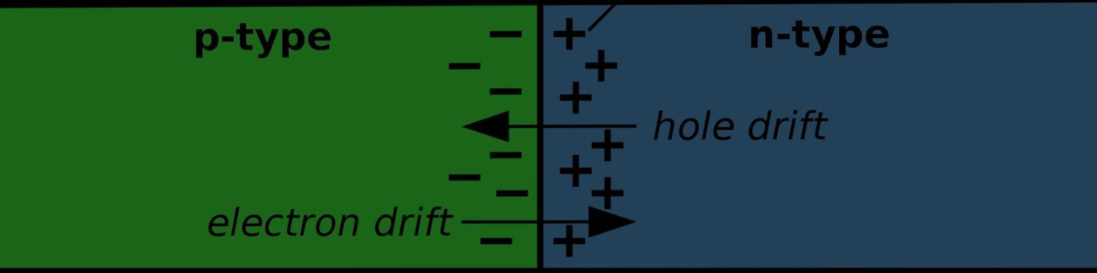
Due to this positive charge region on n-side and negative charge region on p-side of the junction, an electric field directed from positive charge to negative charge develops. Due to this electric field electrons on the p-side moves to the n-side and hole on the n-side moves to p-side. This motion of charge carriers due to the electric field is known as drift current.
Also read -
- NCERT Solutions for Class 11 Physics
- NCERT Solutions for Class 12 Physics
- NCERT Solutions for All Subjects
What is PN junction diode working?
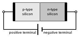
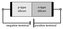
A pn junction diode is nothing but a pn junction provided with metallic contacts at both the ends which are used to supply external voltage to the junction. It is a two terminal device. he pn junction diode and its symbolic representation is shown below.
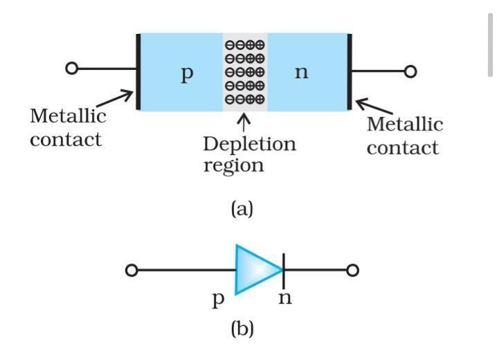
Picture source :- Class 12th physics NCERT (Part-2)
Biasing in PN junction diode
Biasing is a process of connecting the pn junction diode to the battery in order to provide the external input voltage. There are two different types of biasing methods depending upon which of the two terminals of the p-n junction are connected to which of the two sides of the battery.
Forward Bias: When an external voltage V is applied across pn junction diode such that p-side of the pn junction is connected to positive terminal of the battery, n-side of pn junction is connected to the negative side of the battery, then the pn junction is forward biased.
Reverse bias pn junction: When an external voltage V is applied across a pn junction diode such that the p-side of the pn junction is connected to the negative terminal of the battery and n-side of pn junction is connected to the positive side of the battery, then the pn junction is reverse bias pn junction.
Related Topics Link, |
Vi characteristics of diode of pn junction
The Vi characteristics of diode of pn junction is shown below. It represents the change in current with respect to change in voltage or vice-versa. The x-axis represents voltage and the y-axis represents current. The VI characteristics of pn junction can be explained according to three
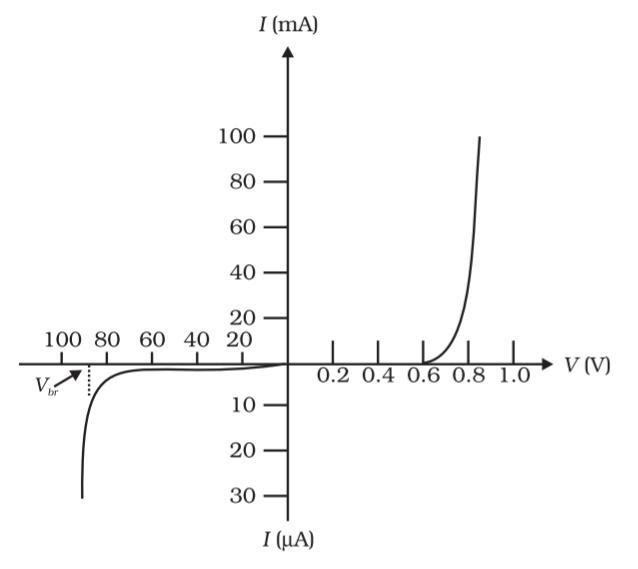
Picture source :- Class 12th physics NCERT (Part-2)
Condition :
Zero bias ? In this condition there is no external voltage is applied, hence the potential barrier is high and the circuit current is 0.
Forward bias ?In the forward bias condition, the external voltage is applied which results in reduced potential barrier and hence the current flows in the circuit.
Reverse bias pn junction ? In the reverse bias pn junction condition, the external voltage is applied but this time potential barrier increases. A small amount of reverse saturation current flows but on increasing the applied voltage, the diode will break.
NCERT Physics Notes:
Applications of PN junction diode
There are some of the common and important application of pn junction diode given below:
It has the potential to be used as a solar cell.
When the pn junction diode is reverse-biased, it can be used as a photodiode because it is sensitive to light.
In forward-biased condition, the pn junction diode can also be used in LED lighting applications.
It is used in many electric circuits as a rectifier because it allows the current to flow only when the circuit is forward biased.
Also check-
Frequently Asked Questions (FAQs)
The current induced when the electrons diffuse from n-side to p-side and holes diffuse from p-side to n-side in the pn junction due to concentration gradient is called diffusion current.
There is a movement of minority charge carriers of p-side and n-side from p ? n and n ? p due to the electric field of charges of depletion region. This motion of charge carriers due to electric field is known as drift current.
When the p-side of the pn junction is connected to positive terminal of battery, n-side of the pn junction is connected to the negative terminal of the battery, then the pn junction is forward biased.
When the p-side of the pn junction is connected to -ve terminal of the battery and n-side of pn junction is connected to the positive terminal of the battery, then pn junction is reverse bias pn junctioned.
In p-type semiconductors doping is done by a trivalent element and holes are majority charge carriers. Whereas, in n-type semiconductors doping is done by a pentavalent element and electrons are majority charge carriers.
A thin layer on both p and n side of pn junction which consist of ionized immobile negative and positive ions left behind by electrons and holes during diffusion is known as depletion region.
Also Read
19 Sep'24 10:29 PM
19 Sep'24 01:53 PM
19 Sep'24 01:25 PM
19 Sep'24 11:15 AM
18 Sep'24 06:06 PM
04 Sep'24 12:24 AM
03 Sep'24 09:36 PM
03 Sep'24 09:30 PM
03 Sep'24 09:28 PM
20 Aug'24 03:03 PM
Articles
Download Careers360 App's
Regular exam updates, QnA, Predictors, College Applications & E-books now on your Mobile

300M+
Students

36,000+
Colleges

550+
Exams

1500+
E-Books

16000+
Certifications
