To draw the I-V characteristics curve of P-N junction In forward bias

To draw the I-V characteristics curve of P-N junction In forward bias

Edited By Vishal kumar | Updated on Jul 02, 2025 07:30 PM IST

The I-V characteristics curve of a P-N junction diode in forward bias is essential for understanding its behaviour in electronic circuits. In forward bias, the positive terminal of the power source is connected to the P-type material, and the negative terminal is connected to the N-type material. This configuration reduces the potential barrier at the junction, allowing current to flow through the diode. The resulting I-V curve illustrates how the current through the diode increases as the forward voltage is applied. Initially, the current remains very low until the forward voltage reaches a certain threshold, known as the forward voltage drop, at which point the current increases rapidly. This characteristic is fundamental in designing circuits that use diodes for rectification and signal processing.

This Story also Contains
  1. Aim
  2. Apparatus
  3. Theory
  4. Diagram
  5. Procedure
  6. Calculations
  7. Result
  8. Solved Examples Based on the I-V Characteristics Curve of P-N Junction In Forward Bias
  9. Summary

Aim

To draw the I-V characteristic curve of a p-n junction in forward bias

Apparatus

A p-n junction (semi-conductor) diode, a 3-volt battery, a 50-volt battery, a high resistance rheostat, one 0.3 volt voltmeter, one 0.50 volt voltmeter, one 0-100 mA ammeter, one $0.700 \mu \mathrm{A}$ ammeter, one-way key, connecting wires and pieces of sandpaper.

Theory

Forward bias characteristics. When the p-section of the diode is connected to the positive terminal of a battery and the n-section is connected to the negative terminal of the battery then the junction is said to be forward-biased. With the increase in bias voltage, the forward current increases slowly in the beginning and then rapidly. At about 0.7 V for Si diode (0.2 V for Ge), the current increases suddenly. The value of forward bias voltage, at which the forward current increases rapidly, is called cut-in voltage or threshold voltage.

Diagram

Procedure

1. Make a circuit diagram as shown in the diagram.
2. Make all connections neat, clean and tight.
3. Note the least count and zero error of the voltmeter (V) and milli-ammeter (mA).
4. Bring moving contact of the potential divider (rheostat) near the negative end and insert the key K. Voltmeter Vand milli-ammeter mA will give zero reading.
5. Move the contact a little towards the positive end to apply a forward-bias voltage $\left(V_{\mathrm{F}}\right)$ of 0.1 V current remains zero.
6. Increase the forward-bias voltage up to 0.3 V for the Ge diode. The current remains zero, (it is due to the junction the potential barrier of 0.3 V ).
7. Increase VF to 0.4 V . Milli-ammeter records a small current.
8. Increase $V_{\mathrm{F}}$ in steps of 0.2 V and note the corresponding current. Current increases first slowly and then rapidly, till $\mathrm{V}_{\mathrm{F}}$ becomes 0.7 V .
9. Make $V_F=0.72 \mathrm{~V}$. The current increases suddenly. This represents the "forward break-down" stage.
10. If the $V_F$ increases beyond the forward breakdown stage, the forward current does not change much. Now take out the key at once.

Calculations

For forward-bias
Plot a graph between forward-bias voltage $V_F($ column 2$)$ and forward current if (column 3$)$ taking $V_F$ along $x$-axis and If along $Y$-axis.This graph is called the forward-bias characteristic curve a junction diode.

From the graph, For a change from point $A$ to $B$

$
\Delta V_F=2.4-2.0=0.4 \mathrm{~V}, \Delta I_F=30-20=10 \mathrm{~mA}
$
Hence junction resistance for forward bias,

$
r=\frac{\Delta V_F}{\Delta I_F}=\frac{0.4 \mathrm{~V}}{10 \mathrm{~mA}}=40 \text { ohms }
$

Result

The junction resistance for forward bias is 40 ohms.

Solved Examples Based on the I-V Characteristics Curve of P-N Junction In Forward Bias

Example 1: Find the value of junction resistance (in ohms) if the change in forward voltage is from 1.4 V to 2.0 V and the change in forward current is from 10 mA to 20 mA.

1) 60

2)20

3)30

4)50

Solution

$r=\frac{\Delta V_F}{\Delta I_F}=\frac{0.6 \mathrm{~V}}{10 \mathrm{~mA}}=60 \Omega$

Hence, the answer is (60).

Example 2: The reverse biasing in the junction diode

1) Increase the potential barrier

2) Increase the number of minority charge carrier

3) Increase the number of majority charge carriers

4) Decrease the potential diode

Solution

To draw I-V characters of P-N junction in reverse biased

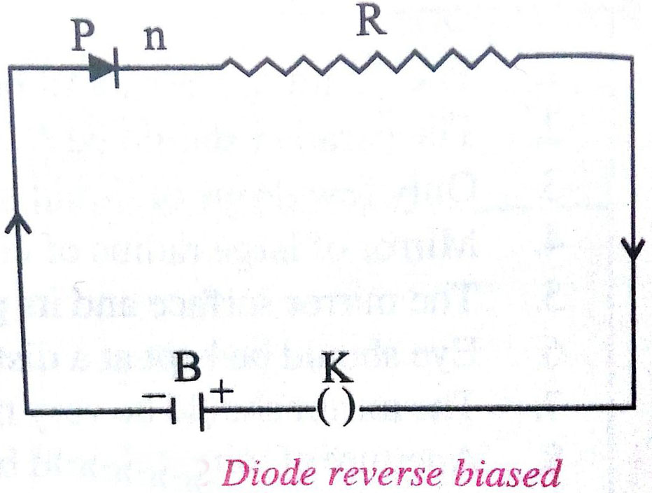
The process by which, a p-n junction diode blocks the electric current in the presence of applied voltage is called reverse biased p-n junction diode.

In reverse biased p-n junction diode, the positive terminal of the battery is connected to the n-type semiconductor material and the negative terminal of the battery is connected to the p-type semiconductor material.

Hence the answer is Option (1).

Summary

The I-V characteristics curve of a P-N junction diode in forward bias shows the relationship between the applied voltage and the resulting current. When the diode is forward-biased, the current remains minimal until the forward voltage exceeds a specific threshold. Once this threshold is crossed, the current increases sharply with small increases in voltage. This curve is crucial for understanding how diodes conduct electricity and for designing circuits that require precise control of current and voltage.

Frequently Asked Questions (FAQs)

1. What is the purpose of drawing an I-V characteristic curve for a P-N junction diode?
The I-V curve helps visualize and understand the diode's behavior under different voltage conditions. It shows the relationship between current and voltage, including the threshold voltage and how current changes with increasing voltage.
2. What is the importance of maintaining a constant temperature during the I-V characteristic measurement?
Temperature affects the I-V characteristics of a diode. Maintaining a constant temperature ensures that the observed changes in current are due to voltage variations alone, allowing for accurate characterization of the diode's behavior.
3. What equipment is typically needed to draw the I-V characteristics curve?
The basic equipment includes a P-N junction diode, a variable DC power supply, an ammeter, a voltmeter, connecting wires, and a breadboard or circuit board for connections.
4. How can you determine the dynamic resistance of the diode from the I-V curve?
The dynamic resistance is the inverse of the slope of the I-V curve at any point. It can be calculated by taking the ratio of a small change in voltage to the corresponding change in current (ΔV/ΔI) at that point.
5. How can you estimate the ideality factor of a diode from its I-V characteristics?
The ideality factor can be estimated by analyzing the slope of the ln(I) vs. V plot in the exponential region of the I-V curve. An ideal diode has an ideality factor of 1, while real diodes typically have values between 1 and 2.
6. What is the significance of the reverse saturation current in the diode equation?
The reverse saturation current (Is) is a key parameter in the diode equation. It represents the current that flows due to minority carriers when the diode is reverse biased and affects the overall shape of the I-V curve.
7. What is the importance of the scale used when plotting the I-V characteristics?
The choice of scale is crucial for accurately representing the diode's behavior. A linear scale is often used for the voltage axis, while a logarithmic scale for the current axis can help visualize the exponential nature of the current increase.
8. How does the width of the depletion region change as the forward bias voltage increases?
As the forward bias voltage increases, the width of the depletion region decreases. This reduction in the depletion region width allows more current to flow through the diode.
9. How does the I-V curve of a Zener diode differ from that of a regular P-N junction diode?
A Zener diode's I-V curve shows a sharp increase in reverse current at a specific reverse voltage (Zener voltage), unlike regular diodes. In forward bias, it behaves similarly to a standard diode.
10. What is the relationship between the I-V characteristics and the energy band diagram of a P-N junction?
The I-V characteristics reflect the changes in the energy band diagram. As forward bias increases, the potential barrier decreases, aligning with the rapid current increase seen in the I-V curve.
11. What is the significance of the breakdown region in the I-V characteristics?
The breakdown region, typically seen in reverse bias, indicates the voltage at which the diode's ability to block current in the reverse direction fails. This is important for understanding the diode's limitations and reverse voltage tolerance.
12. How can you use the I-V characteristics to compare the performance of different diodes?
By comparing the threshold voltages, forward voltages at specific currents, reverse leakage currents, and the steepness of the forward characteristic, you can evaluate and compare the performance of different diodes.
13. How does the I-V characteristic curve help in selecting the appropriate diode for a specific application?
The I-V curve provides information on the diode's forward voltage drop, maximum current handling capability, reverse leakage current, and breakdown voltage. This helps in selecting a diode that meets the specific requirements of an application.
14. Why is it important to use a variable DC power supply in this experiment?
A variable DC power supply allows you to gradually increase the voltage across the diode, enabling you to observe and measure the current at different voltage levels, which is essential for plotting the I-V curve.
15. How should the ammeter and voltmeter be connected in the circuit?
The ammeter should be connected in series with the diode to measure the current flowing through it. The voltmeter should be connected in parallel across the diode to measure the voltage across it.
16. What precautions should be taken when connecting the diode in the circuit?
Ensure the diode is connected with the correct polarity (anode to positive, cathode to negative). Use a current-limiting resistor to protect the diode from excessive current. Avoid exceeding the diode's maximum ratings.
17. Why is it important to limit the current through the diode during the experiment?
Limiting the current prevents damage to the diode from excessive heat generation. It also ensures that the measurements are taken within the diode's safe operating range.
18. How can you use the I-V characteristics to determine the maximum power dissipation of the diode?
The maximum power dissipation can be determined by finding the point on the I-V curve where the product of current and voltage is highest. This typically occurs at higher current levels in the forward bias region.
19. How does the I-V characteristic curve of a P-N junction in forward bias differ from reverse bias?
In forward bias, the I-V curve shows a rapid increase in current after a certain threshold voltage. In reverse bias, the current remains very low until breakdown voltage is reached. The forward bias curve is the focus of this experiment.
20. How does temperature affect the I-V characteristics of a P-N junction diode?
Increasing temperature generally lowers the threshold voltage and increases the current for a given voltage. This can shift the I-V curve slightly to the left and make it steeper.
21. How does the I-V curve of a germanium diode differ from that of a silicon diode?
Germanium diodes typically have a lower threshold voltage (around 0.2-0.3 V) compared to silicon diodes (0.6-0.7 V). The curve for a germanium diode will start to rise at a lower voltage.
22. How does the doping concentration affect the I-V characteristics of a P-N junction diode?
Higher doping concentrations generally lead to lower threshold voltages and steeper I-V curves. This is because more charge carriers are available to conduct current once the barrier is overcome.
23. Why is the forward resistance of a diode not constant?
The forward resistance of a diode varies with the applied voltage and current. As the voltage increases, more charge carriers can cross the junction, effectively reducing the resistance.
24. What is the typical threshold voltage for a silicon P-N junction diode?
The typical threshold voltage for a silicon diode is around 0.6 to 0.7 volts. This can vary slightly depending on the specific diode and operating conditions.
25. What is the difference between static and dynamic resistance of a diode?
Static resistance is the ratio of voltage to current at a specific operating point (V/I). Dynamic resistance is the ratio of a small change in voltage to the resulting change in current (ΔV/ΔI) at a given operating point.
26. What is a P-N junction diode?
A P-N junction diode is a semiconductor device made by joining P-type and N-type semiconductor materials. It allows current to flow easily in one direction (forward bias) but restricts flow in the opposite direction (reverse bias).
27. What does "forward bias" mean for a P-N junction diode?
Forward bias refers to the condition where the positive terminal of a voltage source is connected to the P-type region and the negative terminal to the N-type region. This reduces the depletion region and allows current to flow through the diode.
28. What is the significance of the knee voltage or threshold voltage in the I-V curve?
The knee voltage, also called the threshold voltage, is the point on the curve where the current starts to increase rapidly. It represents the minimum voltage required for the diode to conduct significantly.
29. Why does the current increase rapidly after the threshold voltage is reached?
After the threshold voltage, the potential barrier of the depletion region is overcome. This allows for a significant increase in the number of charge carriers crossing the junction, resulting in a rapid current increase.
30. What causes the slight curvature in the I-V characteristic before the knee voltage?
The slight curvature is due to a small number of charge carriers having enough energy to overcome the potential barrier even at voltages below the threshold. This results in a small current flow.
31. What is the importance of the reverse recovery time in relation to the I-V characteristics?
Reverse recovery time, while not directly visible in the DC I-V curve, affects how quickly a diode can switch from forward to reverse bias. This is crucial in applications where the diode needs to switch rapidly.
32. What is the significance of the saturation current in the I-V characteristics?
The saturation current is the small reverse current that flows when the diode is reverse biased. It's typically very small and relatively constant until the breakdown voltage is reached.
33. How does the I-V curve change if the diode is damaged or defective?
A damaged diode may show abnormal characteristics such as excessive reverse current, a shift in threshold voltage, or non-exponential behavior in the forward region. The curve may appear distorted or irregular compared to a healthy diode.
34. How does the series resistance of the diode affect the I-V characteristics at high currents?
At high currents, the series resistance causes a deviation from the ideal exponential behavior. The I-V curve becomes more linear as the voltage drop across the series resistance becomes significant.
35. How does light affect the I-V characteristics of a P-N junction diode?
Light incident on a P-N junction can generate electron-hole pairs, increasing the reverse current. This effect is more pronounced in specially designed photodiodes but can be observed to some extent in regular diodes as well.
36. What is the significance of the slope of the I-V curve in the forward bias region after the knee voltage?
The slope of the curve in this region represents the conductance of the diode. A steeper slope indicates lower dynamic resistance and higher conductance, meaning the diode conducts current more easily.
37. What causes the slight variation in threshold voltage among diodes of the same type?
Slight variations in doping levels, junction temperature, and manufacturing processes can cause small differences in threshold voltage among diodes of the same type.
38. How does the capacitance of a P-N junction diode change with applied voltage, and how might this affect the I-V characteristics?
The junction capacitance decreases as the reverse bias voltage increases. While this doesn't directly affect DC I-V characteristics, it can influence the diode's behavior in AC circuits and high-frequency applications.
39. How can you use the I-V characteristics to detect if a diode has been reverse-engineered or counterfeited?
Genuine diodes from a manufacturer typically have consistent I-V characteristics. Significant deviations in threshold voltage, reverse current, or overall curve shape can indicate a counterfeit or improperly manufactured diode.
40. What is the significance of the cut-in voltage in the I-V characteristics, and how does it relate to the built-in potential of the P-N junction?
The cut-in voltage, visible as the point where current starts to increase noticeably, is related to the built-in potential of the P-N junction. It represents the external voltage needed to overcome the internal potential barrier.

Articles

Back to top