PN Junction Full Form
What is the full form of PN Junction?
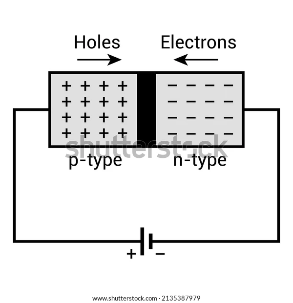
The term PN junction diode refers to a two-terminal or two-electrode semiconductor (namely the p-type and the n-type) device that permits electric current to flow only in one way while blocking the opposite or reverse direction. As a result of this, the current can flow under the condition of forward bias. On the other hand, it obstructs the flow of electricity under conditions of reverse bias.
In this article further, we will see more about PN junction.
Full Form of PN Junction
In PN junction P stands for positive and N stands for negative i.e., positive negative junction. The positive side contains more holes and the negative side contains more electrons. The name PN junction was given by American physicist Russell Ohl of Bell Laboratories in 1939.

Symbol of PN Junction Diode
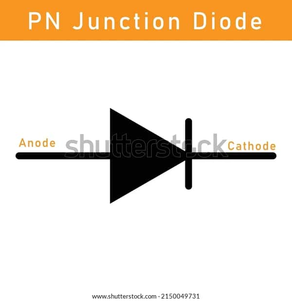
The triangle that points in the direction of a line or passes through one of its vertices is used as the PN junction diode's symbol. With this configuration, the circuit's current flows from the positive anode terminal to the negative cathode terminal.

Formation of PN Junction
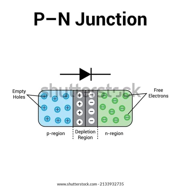
The PN junction is a border or interface that exists between P-type and N-type semiconductor materials within a semiconductor device. In contrast to the N-side, or negative side, of a semiconductor, which has more electrons, the P-side, or positive side, includes more holes. The doping process in a semiconductor produces the PN junction. This technique creates a semiconductor device called a PN junction diode, which is used to enable electric current to flow in one direction while blocking it in the other.

Working Principle of PN Junction
When an electron diffuses from the N-side to the P-side in a PN junction diode, an ionised donor is left behind on the N-side and a layer of positive charge forms on the junction's N-side. Similarly, a layer of negative charges builds up on the P-side of the junction when a hole goes from the P-side to the N-side and an ionised acceptor is left behind. This zone of positive and negative charge on either side of the junction is referred to as the depletion area. In this depletion area, an electric field forms with a direction from a positive charge to a negative charge.

Properties of PN Junction
These are some of the typical characteristics of a PN junction diode:
A PN junction is formed by the joining of two semiconductor regions, one positively doped with a P-type material and the other negatively doped with an N-type material. The PN junction exhibits several unique electrical and optical properties that make it a fundamental building block of many electronic devices. Some of the key properties of PN junctions are:
Rectification: The PN junction allows current to flow easily in one direction while restricting current flow in the opposite direction. This is known as rectification and is the basis for the operation of diodes.
Barrier potential: The junction between the P and N regions creates a potential barrier, which impedes the flow of current in the reverse direction. The magnitude of this potential barrier depends on the doping concentration and temperature of the material.
Forward bias: When a positive voltage is applied to the P-region and negative voltage to the N-region, the potential barrier is reduced, allowing current to flow easily in the forward direction.
Reverse bias: When a negative voltage is applied to the P-region and a positive voltage to the N-region, the potential barrier increases, restricting the flow of current in the reverse direction.
Depletion region: When the PN junction is formed, a depletion region is created near the junction due to the migration of free electrons and holes. The width of the depletion region depends on the doping concentration and applied voltage.
Junction capacitance: The PN junction acts as a capacitor, with the depletion region acting as the dielectric. The capacitance of the junction depends on the width of the depletion region and the doping concentration of the material.
Photovoltaic effect: When light is incident on the PN junction, it generates electron-hole pairs which can be collected as a current. This is the basis of the photovoltaic effect, which is used in solar cells.
Avalanche breakdown: When the reverse voltage applied to the junction exceeds a certain value, the potential barrier breaks down and a large amount of current flows. This is known as avalanche breakdown and can damage the junction if it occurs beyond its safe operating limits.
Zener breakdown: When a reverse voltage is applied to the junction, the potential barrier can also break down due to the Zener effect, which is a quantum mechanical effect. This breakdown occurs at a lower voltage than avalanche breakdown and is used in Zener diodes to provide a stable voltage reference.
Applications of PN Junction
Here are a few of the most intriguing uses for PN diodes:
The PN junction diode is used as a voltage doubler, triple, and quadruple in
various multiplier circuits and also as a switch in an electrical circuit.
These are employed as varactors for voltage-controlled oscillators and multiple circuit rectifiers.
A photodiode is a special kind of p-n junction that consumes light energy to generate electric current.
A Light-emitting diode (LED) is a special kind of heavily doped p-n junction which under forward bias emits spontaneous radiation(light).
It can be used as a detector for the demodulation circuit because it is used in both detectors as well as in demodulators.
Temperature sensors and other devices are made by using the voltage across PN junction diodes.
Frequently Asked Questions (FAQs)
In a forward-biased P-N junction, the current through the junction increases as the battery voltage rises.
Zener breakdown and avalanche breakdown are the two breakdown mechanisms.
Light emitting diode, Zener diode, photodiode and solar cells are mainly the types of PN junction diodes present.
The materials used are purposely formed by adding impurities to semiconductors like Silicon.

